PCB Design for Assembly – SMT / Through-Hole
Overview
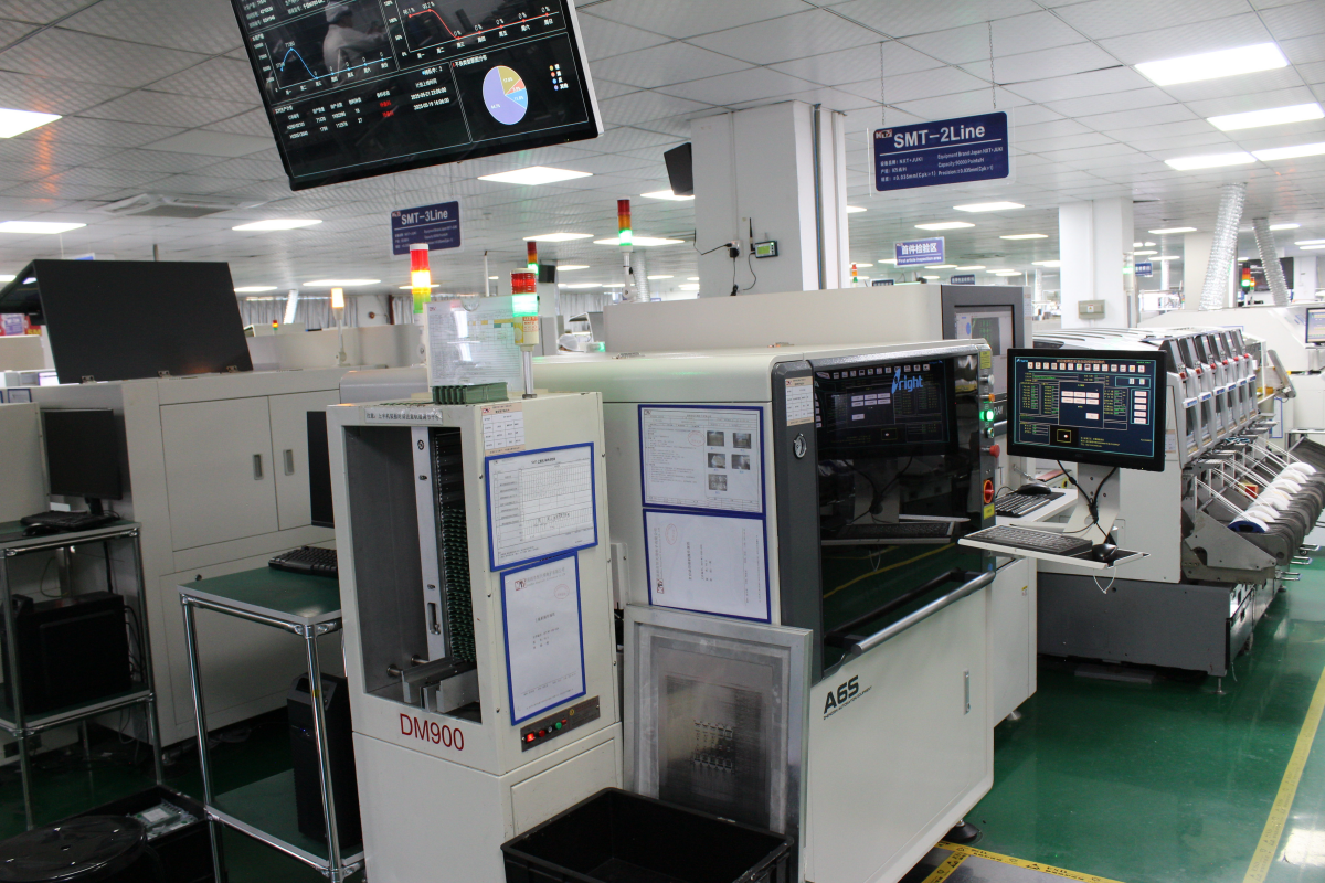
Modern PCBs increasingly combine SMT components for high-density circuits and through-hole components for mechanical strength and connectors. This mixed-technology assembly presents unique design challenges—placement order, soldering compatibility, and thermal management. Studio Electronics offers PCB Design for Assembly covering both SMT and through-hole technologies. As a premier provider of PCB assembly in China, our professional PCB layout engineers design layouts that accommodate both SMT and through-hole components efficiently, ensuring reliable soldering and high-yield assembly. Our 12 automated SMT lines and automatic wave soldering capability support mixed-technology boards from prototype to production.
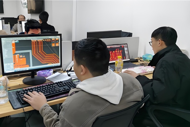
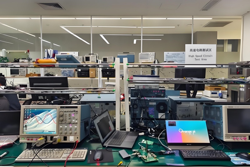
Mixed-Technology Design – SMT & Through-Hole
| Design Consideration |
SMT Optimization |
Through-Hole Optimization |
| Component Placement |
Optimized for pick-and-place efficiency |
Spaced for wave soldering clearance |
| Pad Design |
Optimized for reflow soldering |
Optimized for wave soldering |
| Thermal Management |
Even heating for all SMT components |
Thermal relief for THT connections |
| Assembly Sequence |
SMT placed first; THT inserted after |
Designed for assembly order efficiency |
| Solder Joint Reliability |
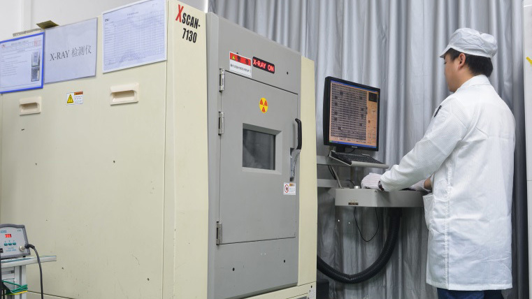
X-Ray inspected for BGA/QFN |
Wave soldered for reliable mechanical joints |


Our Design-for-Assembly Process
Stage 1: Technology Assessment
We review your design requirements and determine the optimal mix of SMT and through-hole technologies. Component selection considers both electrical performance and assembly compatibility.
Stage 2: Layout with Assembly in Mind
Our PCB layout engineers position components to optimize assembly:
-
SMT components on primary side where possible
-
Through-hole components placed for wave soldering compatibility
-
Adequate spacing for soldering and inspection
-
Thermal copper balancing for even reflow
Stage 3: Design Review
A systematic assembly review verifies:
-
Component clearance for placement tools
-
Solder pad design for both reflow and wave soldering
-
Thermal management for mixed technology
-
Test point accessibility
Stage 4: Prototype Build & Validation
We fabricate 5-10 samples and assemble them on our 12 automated SMT lines. Through-hole components are processed through automatic wave soldering. Prototypes undergo AOI, X-Ray, and functional testing. Samples are shipped to you for confirmation.
Stage 5: Production
After approval, we scale to production—handling low volume PCB assembly or high-volume orders with the same mixed-technology expertise.

Why Design for Assembly Matters
-
Higher Yield – Designs that match assembly processes
-
Lower Cost – Efficient assembly reduces cost
-
Reliable Soldering – Optimized for both SMT and through-hole
-
Faster Production – Smooth assembly flow
-
Mixed-Technology Support – Comprehensive capability for any board type
Studio delivers PCB Design for Assembly—SMT and through-hole optimized for reliable, high-yield production.


